Hackerspace News
News
Les samedis matins : Café Créatif du C01N et du CREDO – un atelier de découverte et d’expérimentation en fablab à partir du 14 mars 2026
Découverte, initiation, expérimentation … Les samedis matins, venez vous initier à des techniques et des pratiques numériques, artisanales ou artistiques à travers la réalisation de projets collectifs ludiques et créatifs. Vous pourrez découvrir par exemple les logiciels de création graphique (dessin, retouche d’images, modélisation), les machines à commande numérique (imprimante 3D, découpe/graveuse laser, brodeuse), les machines textiles (machine à coudre, surjeteuse, brodeuse, tricoteuse), les bases de l’électronique, et bien d’autres choses encore. … toutes les possibilités d’un fablab pour exprimer sa créativité ! Pour mettre en œuvre cette initiation, nous choisirons ensemble des petits projets à la croisée de ces pratiques. Nous pourrons par exemple fabriquer un puzzle (retouche d’image, dessin vectoriel, découpe laser), un agenda ou un carnet de notes personnalisé (traitement de texte ou dessin vectoriel, micro-édition, textile, plotter ou laser pour la couverture), un jeu de plateau avec figurines (dessin vectoriel, découpe laser, modélisation 3D, impression 3D, textile pour ranger les figurines), un jeu vidéo (moteur de jeu vidéo, outils graphiques, outils sonores), une lampe de poche (électronique, modélisation 3D, impression 3D), etc. Organisation des ateliers La première séance sera consacrée à une visite des espaces dédiés (fablab Atelier du C01N et espace multi-activités CREDO) pour découvrir les matériels, machines, outils et fournitures mis à disposition, et un temps d’échange sur les envies de chacun·e et les propositions de projets à réaliser collectivement ou individuellement. Nous déciderons ensemble d’un calendrier des séances suivantes à programmer au moins 2 samedis matins par mois. Cette première séance est programmée le samedi 14 mars 2026, de 10h à 13h. Rendez-vous au CREDO (salle D12 du 108 Maison Bourgogne). C 4 : la créativité puissance 4 ! Café … C’est tout à la fois un moment où l’on se rencontre, où l’on partage … … Créatif … … ses idées, sa créativité, où l’on invente et fabrique ensemble … … du C01N … … en utilisant les machines et outils de l’Atelier du C01N (espace fablab) … … et du CREDO … et ceux du CREDO (espace multi-activités). Pratique Cet atelier est destiné aux personnes qui souhaitent se familiariser avec les activités d’un fablab. Il se déroule les samedis matins de 10h à 13h , au moins deux fois par mois, à l’Atelier du C01N (salle D2) et au CREDO (salle D12) situés au 3ème étage du 108 Maison Bourgogne. Vous pouvez venir avec votre ordinateur portable ; quelques PC d’atelier seront disponibles sur place. Cet atelier est gratuit et ouvert aux adhérent·es de l’association La Labomedia (20€/an) ; toutefois la première séance est libre d’adhésion (séance d’essai). Il est possible d’adhérer sur place. L’article Les samedis matins : Café Créatif du C01N et du CREDO – un atelier de découverte et d’expérimentation en fablab à partir du 14 mars 2026 est apparu en premier sur Labomedia .
Famikey or: How I Learned to Stop Worrying and Love the Membrane
CRASH Space welcomes guest writer Lucas Leadbetter as he shares his recent love for keyboards with the CRASH community For anyone that knows me, you know that I absolutely love computer keyboards, specifically mechanical ones. I’ve always been enthralled by them, the tactility and usefulness makes me enjoy using them and collecting them. But more than that, I love finding the most unique and absurd keyboards, ones that push the limits of what is useful. And that leads me to my most recent project: a USB-compatible Family BASIC keyboard, originally for the Famicom. But… why? Simply put: I just thought it’d be neat. I stumbled upon the keyboard in a used game shop in Brooklyn, and as soon as I saw it I realized I wanted to make it compatible with a PC. The keyboard itself is so unique, and the fact the badge says “Nintendo” on it and is legitimately a Nintendo product is fascinating as a computer peripheral! But the bigger problem was that I had zero practical experience with writing microcontroller code, especially as it pertains to more complex (ish) things like keyboard matrixes and scanning for updates. What is Family Basic? Taking a step back, Family BASIC was a product designed for the Family Computer (widely known as the Famicom) to enable users to build games in BASIC (Beginner’s All-Purpose Symbolic Instruction Code) for the console. The original packaging The product itself came with the cartridge for the Famicom as well as the noted keyboard. See Wikipedia for a bit more info. What is to note is that the layout of the keyboard is specifically designed with BASIC in mind, with specific keys noted for that purpose, which means that it can be kludgy to use with modern PCs. Preparation Before getting started, I did a lot of research. I bought a keyboard, but the next step was to find out what exactly would be needed to make this work. The keyboard is from a release in 1984- so much of what I’m working with is relatively old tech (40+ years old at this point), so being cautious was paramount as to not ruin vintage tech. During that preparation, I found a bunch of information across the internet, but nothing centralized. NESdev Wiki One of the biggest sources of information (which is also used by the next source) was the NESdev Wiki. Specifically this resource . This included a lot of information about the layout and technical implementation, and was actually where I initially started to ponder the implementation of the microcontroller code. Importantly, it also includes the column and row information which is helpful beyond words, as well as links at the very bottom to the keyboard schematics, which is also infinitely helpful (and will come up soon!). CircuitRewind’s Implementation CircuitRewind actually beat me to the punch here. He had a video on this exact topic . And most importantly, he also open sourced his code for the matrix polling logic, designed for the RP2040 microcontroller. This was invaluable – it gave me an immediate start point, including pinouts that could be used to solder up the microcontroller to a cut-up DA-15 expansion connector. I cannot thank him enough for this, and putting this out in the world, and I highly, highly recommend checking his channel out. For a smaller channel, this niche project had a concrete answer that it was both possible and was already done. So while this project wasn’t going to be a 1 of 1, it could at least be a 1 of 2. Internal Photos The one thing that eluded me for a long time was the lack of any good photos of the internals of the keyboard. CircuitRewind’s video was a great source for many things, and it actually got me into one important design decision I’ll talk about later, but it didn’t show the internals clearly at times as it was likely cut for purposes of making good content- but for my purposes, it was lacking. After much digging, I came across two different places with good to great photos. The first being this blog from 2019 . And the second being this post from Emu-Land’s forum from 2018 . The latter of which is what actually got me what I needed: concrete answers to what is going on in the inside, how the keyboard works from the POV of a mechanical keyboard enthusiast, and high-resolution photos of the connectors as well. These photos confirmed what I had figured- it was an early 80s membrane keyboard, so it’d feel awful to type on, but the actual mechanics were relatively simple and there was a real PCB in the shell. Planning Now that I had information, I could start to formulate a plan of attack. As I had mentioned prior, the one thing that the CircuitRewind’s video showed me was that the DA-15 cable was not, in fact, soldered onto the board, but rather a plug into the PCB, meaning it could be possible (in theory) to do a non-destructive mod where it would just be a simple microcontroller, a USB cable, and some sort of adapter, and you could always return it to be the Family BASIC keyboard for the Famicom. This became my biggest goal, in fact. In all reality, it’s likely that I won’t ever need to revert it back to a Famicom keyboard, but there is an element here that preserving tech history is very important, and destroying even a piece of a relatively obscure product (obscure in the states, that is) is not good. Plus it’s cool, ya know? Secondly, it helped the whole project to become easier in some ways, as well as being far more repeatable if any of y’all want to do it as well. I’ll include a BoM lower down if you’d like to do so- should be relatively cheap once you know what you need (I did not, and bought a lot of extra stuff). It took a few weeks for me to get the first of two Family BASIC keyboards in. Why two? Well, I figured I might break the first, so a second would be the pretty one I could use. Spoilers: I didn’t need the second one. Once I got the board, however, I realized that some of the parts I purchased ahead of time that I waited for weren’t correct. But it also did make things a lot easier to do, since the correct parts were readily available. Notably, the connector was specific and very likely out of production. The connector looked like so: Original connector for DA-15 It was a 2.0mm pitch, 11 pin single row connector- not 2.5mm pitch connector as I had assumed. Original DA-15 Cable Reference for the Family Basic Keyboard For reference if you have the original DA-15 connector – this shows the original cable’s wire colors and their functions (physical order, from pin 1 to 11 as noted on the connector’s 1 and 11 markings): Pin Number Original Color DA-15 Pin Function 1 Brown 01 Logic Ground 2 Red 04 Data 4 3 Orange 05 Data 2 4 Yellow 06 Data 3 5 Green 07 Data 1 6 Blue 10 OUT2 (Enable) 7 Purple 11 OUT1 (Col Sel) 8 Gray 12 OUT0 (Reset) 9 White 13 Extra Data (unused for this project) 10 Black 15 Power (VCC) 11 Light Green Chassis Chassis Ground (bypassed DA-15 connector) Build Guide The guide is actually pretty straightforward once you have the right parts, and with everything ready to go, it can take about an hour to mod it, including soldering. Bill of Materials (BoM) Here’s the CSV to download if you’d prefer: bom Download Quantity Name Description Link 1 JST PH 11-pin single-row connector w/ attached leads Used to connect the KB2040 to the DA-15 port; the one linked is a pack of 20, so consider other sources if you can find something cheaper https://www.amazon.com/dp/B0DMZM59QS 1 KB2040 The primary microcontroller; other options may work, but will require source code adjustments https://www.adafruit.com/product/5302 1 26 AWG wire Used to connect ground from KB2040 to the chassis 1 Silicone USB-C to USB-A cable This is pretty much up to you on what the other end is, but I find USB-A to be a little more common with PCs to connect a keyboard to. The only important thing is to have it be silicone to be easily routable. https://www.amazon.com/dp/B0CRZ6KLZM 1 Kapton tape Used to wrap the KB2040 (and soldered pads) so it doesn’t short on the metal chassis; consider a wider width if needed. https://www.amazon.com/dp/B07F8TZZ4N 2 (Optional) Heat shrink/wire caps To cover the end of two extra wires from the connector; alternatively can use Kapton tape or similar to prevent the ends from shorting out. – Soldering Iron – Solder – Wire Strippers Removing insulation from extra wire for chassis ground – Flush Cutters Trimming JST PH connector housing Assembly Now that I had (or you have) all the necessary components, let’s actually get to building. In general, it breaks down into a few steps. Disassembly Disassembling the Family BASIC keyboard is relatively easy. The bottom of the keyboard has 6 screws- 3 on the top and 3 on the bottom. Due to the age of these keyboards, which are now 40+ years old and entirely made of plastic, being careful is really important . The screws go into plastic posts which can shear due to the screws likely never being unscrewed over the years. If the posts do shear, use a little epoxy or and just be careful reassembling (and likely plan on never taking it apart again). Once you’ve unscrewed the base, then carefully pull the bottom off, noting that the DA-15 cable is routed through the bottom case. To get it fully off, you will need to remove the grommet and pull the cable out of the strain relief, unscrew the light green wire from the metal chassis (there’s a spade connector, so it doesn’t need to be unscrewed fully), and then unplug the connector housing from the PCB. The PCB is only fixed in through some plastic posts- the same “be careful” advice applies here, although I never had issues with fragility. Unplugging the connector might be challenging, so using something thin or a plastic spudger can help here. The PCB would look like: Family Basic PCB The DA-15 connects into the P1 slot, which is along the side of the board. I found that keeping the other two connectors attached was easier than fully disconnecting. The grommet is actually reusable, and I’d encourage doing so since it’ll prevent the USB cable from being cut by the plastic, as well as making the install look significantly cleaner. Trim the JST Connector The next step is to take the JST PH connector and trim the back plastic flush against the connector housing using flush cutters. Without this the connector presses a little too much for my liking against the socket backplate, so doing this just makes it a little easier. With that said, I’m also not fussed about the risk of disconnection since we’ll use the strain relief posts to help mitigate the amount of pull on the KB2040, and as a result, the connector itself will experience little pull. Here’s the untrimmed connector: Untrimmed connector housing And a resulting connector: Trimmed connector housing You can test it by plugging the connector in and trimming as needed. Solder the Wires to the KB2040 and Screw Wire to Chassis The next step is the more complicated one, but just because it takes some time. Note: The very first wire (black in this case) is not used. The wire mapping here is mostly to show where to solder the wires and as a mapping to the old connector, so you’ll see there’s an extra. Tape it off, just like the new white cable. The mapping looks like: Original Color Wire Color KB2040 Socket GPIO Function Lt. Green Extra 26 AWG wire (solder to GND pad) GND GND Chassis Ground Black Red 3.3V 3V3 Power (VCC) White White (tape off) – – Not Connected Gray Yellow D2 GP2 OUT0 (Reset) Purple Orange D3 GP3 OUT1 (Col Sel) Blue Green D4 GP4 OUT2 (Enable) Green Blue A0 GP26 Data Pin 1 Yellow Purple A2 GP28 Data Pin 3 Orange Grey A1 GP27 Data Pin 2 Red Brown A3 GP29 Data Pin 4 Brown Black GND GND Ground The wire color is based on the JST PH connectors I purchased (and linked above) . The ordering will be top-down, if the connector faces to the left, like so: JST PH connector wire ordering Next, screw the extra wire (the 26 AWG wire you soldered to GND) to the chassis. At this point, if you’d like to “production-ize” it, you could attach a spade connector like the original cable, or if lazy like me, just strip a little extra cable and wrap around the screw and screw down. Once finished, it’d look like something like this (where the green wire is the extra one I soldered to the KB2040): KB2040 soldered with the ground wire screwed in Lastly, plug the KB2040 into the PCB and you’re done with most of the hard work! Flash the Firmware Next, I flashed the firmware using the source in https://github.com/lleadbet/famicom-keyboard – the README includes a duplication of some info in this post, but the instructions on how to compile the firmware is included. Once you have the .uf2 file, just start the KB2040 in the bootloader via pressing the BOOT button and plugging the KB2040 into a PC using the USB-C cable and paste the file into the newly mounted drive. The KB2040 will restart at that point. Once that’s done, you can test the board. Press a few keys and see if it works- if not, check the wire order and that the board is fully plugged in. Other than that, I have no idea ¯\_ (ツ)_ /¯. After testing, you should also note that it contains VIA support. The GitHub repo includes information on how to set that up, and I’d encourage you to do so- having modern features on a 40+ year old keyboard is a treat. Final Assembly The last steps are to wrap the PCB into Kapton tape, find a spot to put the KB2040, and route the USB cable. Finally, close ‘er up and enjoy your fancy new Family BASIC keyboard on a PC! The Kapton tape should ideally fully wrap the KB2040, as to prevent any part of the board from shorting on the metal chassis. In an ideal world I’d print a 3D part to slot into the case like the original does, but for a mod this feels sufficient, plus Kapton won’t leave residue. I found putting the KB2040 into the top shell like so worked fine. Just note to be careful when routing cables, as it can be easy to pinch them when closing up: KB2040 in its final resting place You can use the existing strain relief posts to route the USB cable as well: Strain relief posts Lastly, here’s how it should look closed up: Family BASIC keyboard with USB cable Summary It works! With a combination of prior work I’ve found as well as some newer approaches, I have a working, USB-C compatible Family BASIC keyboard that can be used with VIA to create custom keymaps/layers. The keyboard isn’t great to use for a daily driver, but as a novelty it’s hard to beat. The membrane sucks to type on… but yet I find it a uniquely enjoyable experience, one that I don’t think I’ve ever had before and still is something I’d love to share with others. GitHub / Source Code All source is available on https://github.com/lleadbet/famicom-keyboard , and includes information on how to use. This post mostly serves as the build guide and context behind the build.
Kiberdrošības treniņš 3.martā Ventspilī
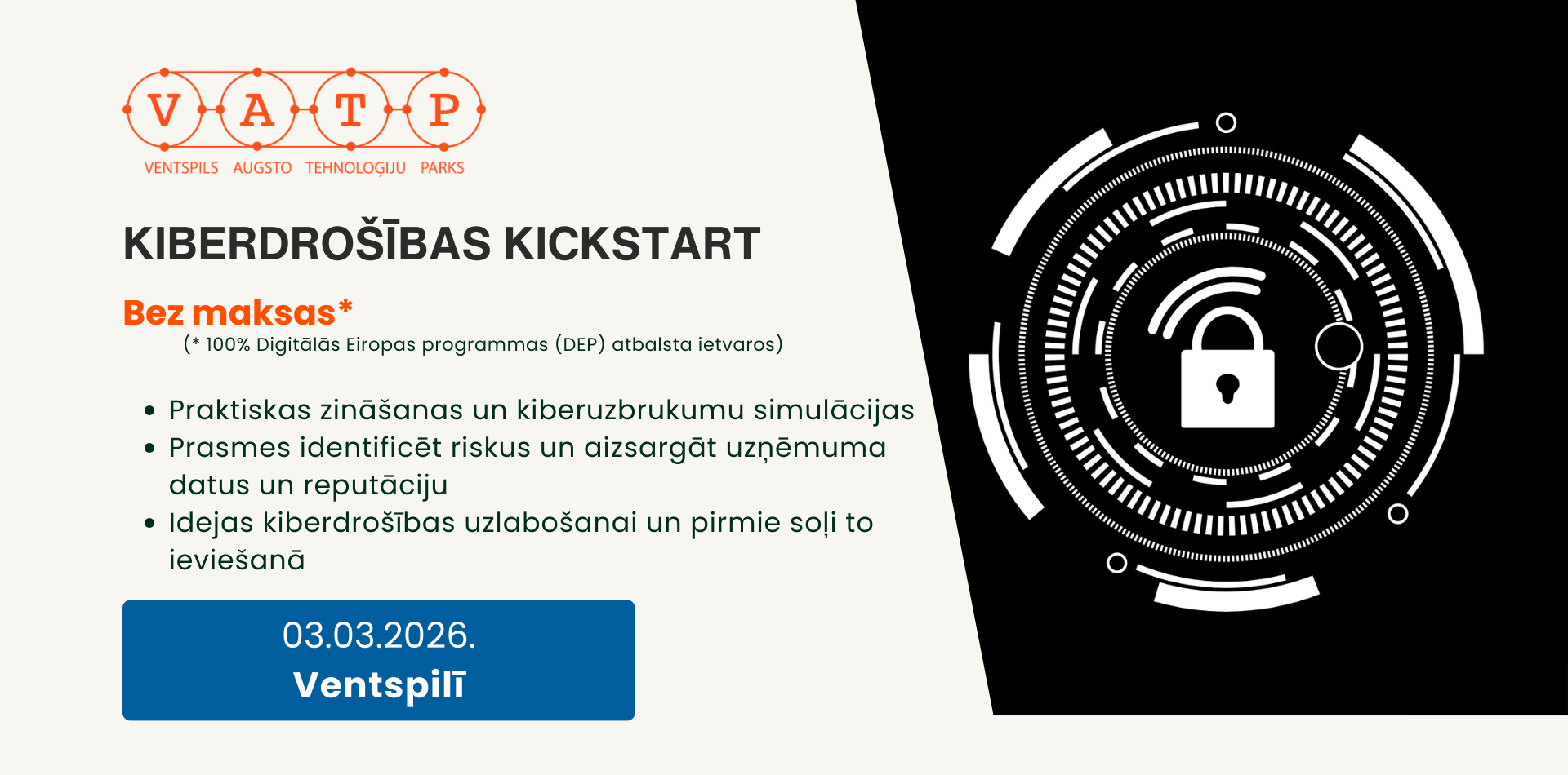
Vai Tavs uzņēmums ir gatavs kiberdrošības izaicinājumiem? Aicinām piedalīties Eiropas Digitālā inovācijas centra (EDIC) interaktīvajā treniņā Kiberdrošības Kickstart. Treniņš radīts sadarbībā ar Norvēģijas partneriem un guvis panākumus Skandināvijā. Šīs apmācības ļaus praktiski piedzīvot kiberuzbrukumu simulācijas un saņemt ekspertu padomus, kā stiprināt uzņēmuma digitālo drošību. Ko iegūsi treniņa laikā: praktiskas zināšanas un kiberuzbrukumu simulācijas; prasmes identificēt riskus un aizsargāt uzņēmuma datus un reputāciju; idejas kiberdrošības uzlabošanai un pirmie soļi to ieviešanā. Pasākuma programma: Ierašanās, reģistrācija Kiberdrošības treniņš Kiberdrošības treniņš (Krists Mediņš - EDIC Digitālo sistēmu pārvaldības speciālists, Zanda Jurgenberga - LMT kiberdrošības eksperte) Kafijas pauze Kiberdrošības higiēna (Guntars Alliks – LMT Kiberdrošības pakalpojuma vadītājs) EDIC pakalpojumi un atbalsta iespējas (Krists Mediņš - EDIC Digitālo sistēmu pārvaldības speciālists) Pasākuma datums un laiks: 2026. gada 3. marts pl. 9:30 - 13:30 Norises vieta: Ventspils (vieta tiks precizēta) REĢISTRĒŠANĀS OBLIGĀTA - https://forms.office.com/e/qEzB0ZkXSa Dalība bez maksas. Vietu skaits ierobežots! Finansējums: 100% Digitālās Eiropas programmas (DEP). Pirms pasākuma nepieciešams aizpildīt digitālā brieduma testu, kas pieejams vietnē: https://tests.edic.lv Apmācības piemērotas maziem un vidējiem uzņēmumiem. Lai pilnvērtīgi piedalītos apmācībās, nepieciešams viedtālrunis. Kontaktpunkts Kurzemē : Ventspils Augsto tehnoloģiju parks Uldis Fridrihsbergs uldis.fridrihsbergs@vatp.lv (LIAA) Deniss Baranovs deniss.baranovs@vatp.lv (LIAA)
Les mercredis après-midi : Goûter Créatif du C01N – un atelier de créativité numérique à partir du 11 mars 2026
Atelier de créativité numérique Les mercredis après-midis, l’Atelier du C01N ouvre ses portes aux adolescent·es à partir de 12 ans pour pratiquer le numérique sous toutes ses formes à travers des activités ludiques. Comprendre les bases de l’algorithmique, découvrir la programmation (divers langages selon la finalité), prendre en main les logiciels de dessin vectoriel, de modélisation 3D, de création sonore, et bien d’autres … le tout en s’amusant, c’est le programme de ces ateliers ! Planning des prochaines séances Mercredi 11 mars : découverte d’Inkscape, un logiciel de dessin vectoriel, avec un mini-jeu coopératif Mercredi 18 mars : initiation à l’algorithmique sans ordinateur, avec quelques défis à résoudre Mercredi 25 mars : initiation à l’algorithmique dans l’interface de programmation graphique libre Scratch, pour créer des mini-jeux vidéos Mercredi 01 avril : découverte d’Inkscape, un logiciel de dessin vectoriel, avec un mini-jeu coopératif Mercredi 08 avril : découverte de Bitsy, un moteur de création de jeu vidéo 2D en pixel art La suite en septembre. Cet atelier est destiné (prioritairement) aux adolescent·es (à partir de 12 ans). Il se déroule les mercredis après-midis de 16h30 à 18h30 , hors vacances scolaires, à l’atelier du c01n (salle D2 au 3ème étage du 108 rue de Bourgogne à Orléans). Cet atelier est gratuit et ouvert aux personnes adhérentes à l’association La Labomedia (20€/an), dans la limite de 6 personnes. Il est possible d’adhérer sur place. Merci de vous inscrire via notre formulaire de contact , en précisant les séances souhaitées. L’article Les mercredis après-midi : Goûter Créatif du C01N – un atelier de créativité numérique à partir du 11 mars 2026 est apparu en premier sur Labomedia .
How to keep data centers from breaking the grid
Originally published on Fast Company , this article by mHUB CEO Haven Allen appears here in full AI ’s explosive growth depends on a backbone of vast energy-hungry, water intensive data centers, costing hundreds of billions of dollars in resources. The challenge—and opportunity—of the moment is ensuring this infrastructure scales without hollowing out long-term value. Across the U.S., states are racing to attract data center facilities with lucrative incentives. The promise is economic growth and prestige. The reality is more complicated: hidden costs borne by communities, power grids, and ecosystems. As a venture capitalist focused on hardtech and sustainability, I see this tension as both risk and opportunity. The future of AI will belong to those who reconcile scale with sustainability, building infrastructure that powers innovation without draining the very resources societies depend on.